
Semiconductors
Vacuum Deposition Equipment & Solutions

The world of semiconductors is constantly and rapidly evolving. New technologies have special requirements which call for customer-oriented, flexible and new solutions.

Semiconductors represent one of the most important building blocks of technology innovation, from single digit nanometer technologies through new materials and technology options.

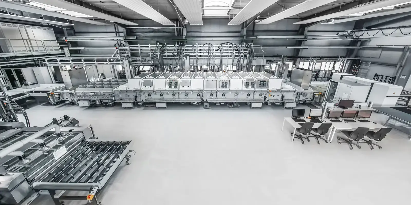
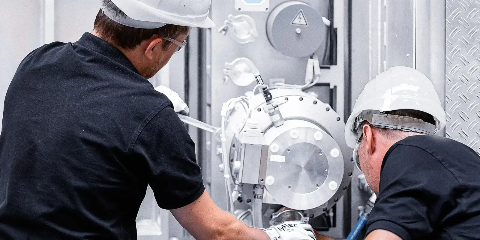
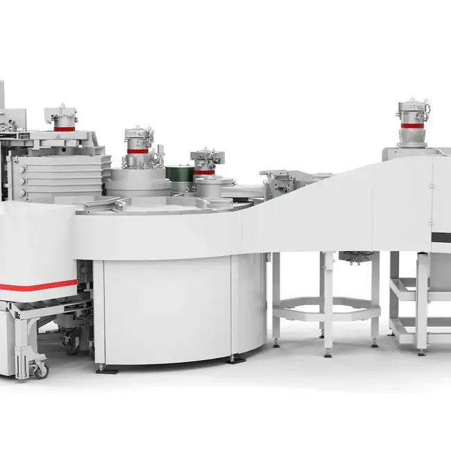
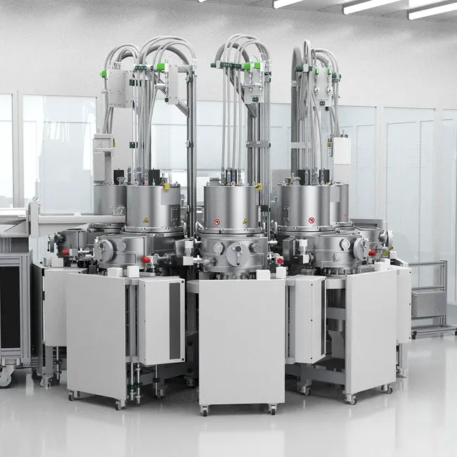
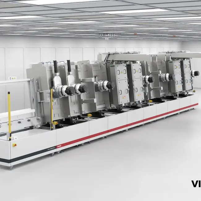
VON ARDENNE offers design, engineering, manufacturing as well as commissioning and service for special deposition equipment and components.

Many years of expertise in the fields of vacuum technology and deposition solutions coupled with a broad network enable excellent project implementation for our customers.

Would you like to learn more? Explore the content below or contact us.

Excellent implementation of new requirements

with a highly experienced team

Customer oriented and flexible

in platform & component development of special technology topics

Cooperation based on partnership

in the long-term project implementation

FAQ

High-precision vacuum deposition equipment, custom engineering, manufacturing, commissioning, and lifecycle service for wafer and panel applications. 

Magnetron sputtering, electron-beam evaporation, thermal evaporation, laser-arc evaporation, and related pretreatment and in-process measurement systems. 

Yes. We tailor platforms and components to specific materials, throughput, and line-integration needs, using a configure-to-order model to accelerate time to value. 

Advanced packaging, MEMS, and PiezoMEMS today, with broader coverage across front-end and back-end semiconductor use cases.

CLEANROOM
  • Production of vacuum coating systems for precision optics, photonic systems and semiconductor applications 
  • Sampling & Pilot Deposition Services 
  • 600 qm Semiconductor Cleanroom including AMC capability 
Support
Media
No news available.
CONTACT
02.09.2026 - 04.09.2026
Semicon Taiwan 2026

Taipeh, Taiwan

Silicon Saxony Pavilion

Search